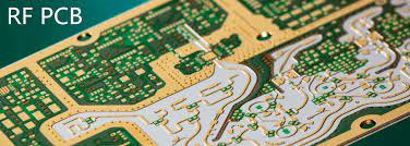
Choose the Appropriate RF PCB Stackup Configuration
When designing an RF PCB, it’s important to understand how the circuit’s layer stackup configuration can impact signal integrity, power distribution, and noise isolation. Engineers must consider the layer count, design flow, and manufacturability when choosing the appropriate RF PCB stackup configuration.
As you can imagine, the higher the layer count of an RF PCB, the more complex it is to manage signal and power distribution. The layers need to be carefully arranged to prevent interference between different circuit blocks, and the layer count needs to be sufficient to provide adequate decoupling of critical signals and components.
In addition, the RF laminate material used for the PCB stack-up must be able to handle high-frequency signal transmissions. This requires a high-quality, low-loss dielectric that can deliver the necessary signal impedance for efficient routing and power delivery.
RF PCBs are characterized by a wide range of varying functionalities. This can include high-speed digital, mixed-signal, and RF devices that require both low-loss signal paths and good power distribution. The challenge comes in effectively consolidating these various functionalities while ensuring that the final product meets performance and cost requirements.
One of the most important aspects of rf pcb design is floorplanning. This is where designers plan out the layout of all the critical signals and traces on the board. The process combines routing, signal and power plane placement, component selection, and circuit optimization to ensure that the overall design meets all requirements. Getting this part of the process right is especially crucial when working at practical RF frequencies because it impacts the performance of the RF device.
How to Choose the Appropriate RF PCB Stackup Configuration
While there are many tools available to help designers determine the ideal trace width for a particular signal, it’s also essential to choose an appropriate laminate material for the stack-up. Different materials have different dielectric constants, loss tangent values, and thermal conductivity properties that can affect the performance of the RF PCB.
The layer stack-up is a vital aspect of RF PCB design, and it is critical that the RF signal layer is positioned at the top followed by the ground plane. This arrangement allows the ground plane to function as a low-impedance return path for the RF signals. This can reduce loop area and thereby minimize the potential for noise and EMI in the circuit.
It’s also important to make sure that the ground planes in your RF PCB are properly connected to the signal and power layers using stitching vias. This helps ensure that the ground planes have a consistent reference potential across the entire RF PCB, and it can also improve decoupling by increasing interplane capacitance. Lastly, you’ll need to make sure that the RF signal and ground layers have appropriate clearances between them to avoid unwanted shorts. By incorporating these key design considerations into your RF PCB, you can create a high-performance, reliable, and cost-effective product.